新闻资讯
联系我们
济南市高新区联合财商广场1号楼15层
联系人:高经理
电 话:0531-85235999
手 机:17156776999
传 真:0531-58702200
网址:www.leilatu.com.cn
 |

济南市高新区联合财商广场1号楼15层
联系人:高经理
电 话:0531-85235999
手 机:17156776999
传 真:0531-58702200
网址:www.leilatu.com.cn
稳压电源LDO也就是线性稳压电路,从应用的输入电压中减去超额的电压,产生经过调节的输出电压。LDO(低压降)稳压器通常使用功率晶体管(也称为传递设备)作为 PNP。本文将浅谈一下关于模拟电路应用之LDO的PSRR计算。
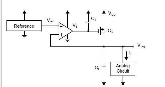
讲讲作者君最近有见过的一个很基本的电路:LDO(A low-dropout or LDO regulator is a DC linear voltage regulator that can regulate the output voltage even when the supply voltage is very close to the output voltage.),就是传说中的无处不在的稳压电路。
作者君捣鼓这个电路的初衷,是看看我调整了input电压之后,PSRR有没有很显著的恶化。因为之前有个别人做好的LDO,但是input是bandgap的1.2V,作者君把input改成0.8V之后,就稍微改了一些东西:比如把之前OTA的input pair从pmos变成了nmos。然后,因为这个LDO的PSRR要求比较高,作者君就小小的捣鼓了一下PSRR的计算。
我们还是从书本来说起吧!
上面的图是来自“Analog Integrated Circuit Design, 2nd EdiTIon,Tony Chan Carusone, David Johns, Kenneth MarTIn”
不管怎么说,我们要考虑一个系统的frequency response特性,首先跑不掉的就是loop gain。 因此,可以按照下面的公式算出loop gain,其中包括两个可以预计到的pole:一个在OTA的output,一个在LDO的output:
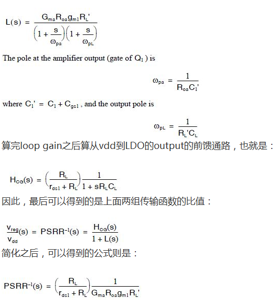
可以看出,DC时候的PSRR其实就是整个system的DC gain的一部分。因此,想得到一个大的PSRR,需要有一个比较大的gain的OTA,这个是可以预料到的。
同时,如果我们考虑上面两个都可以成为主极点的pole的大小,可以用下面的图来解释。
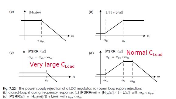
图a是PSRR公式里面的分子部分,也就是前馈部分。然后,图b是分母部分,也就是整个system的loop gain。
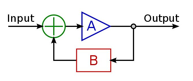
或者说,分子就是这个经典feedback system里面的A,就是从VDD到output的传输函数;然后分母是AB,就是loop gain。
因此,考虑两种不同的情况:LDO的输出是主极点,就得到了图c;OTA的output 是主极点,就得到了图d。
大家应该可以再次感受到了用dB做单位的好处:PSRR的公式就是直接把图a和图b相加的结果!多么简单直观啊!
然后,这样一来,作者君发现:可以用PSRR来判断哪个pole是主极点!OTA的输出是主极点时,PSRR是图d;而LDO的output是主极点的时候,PSRR是图c!哼哼!这样算是“一物多用”吗?
作者君的实际电路是下面这样子的。
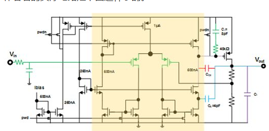
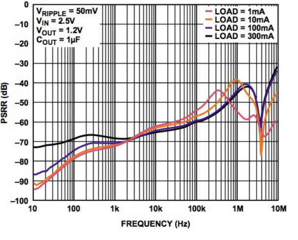
阴影部分就是OTA。如果compensaTIon capacitor只有下图里面红色的miller capacitor Cc0和紫色的CL时,我调整了一下CL的大小,PSRR的simulaTIon results如下图:
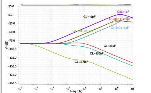
也就是说,想要得到上面那张图7.22(C)里面的完全不向上翘起的结果,你的CL必须相当大。比如,CL要47uF。而此时,miller capacitor才不过1pF而已……大家感受一下数量级的差距。因此,若是有条件接片外电容,大家放心大胆的用。但是若是只能用片上的电容,大家就得小心一些了。
比如:看看大约在1MHz左右,最上面那条紫色的线,居然超过0dB了!也就是说,VDD上面的高频扰动会被放大之后显现在LDO的output上面!
因此,其实作者君拿到的LDO并不是用红色的Cc0来做compensation的,而是加上了蓝色的Cc和绿色的C1。这样一看,OTA的output node(或者说是输出级的power pmos的gate)并没有通过capacitor连接起来。而是,跨过了一个common gate的nmos,Cc才连着output那里。
然后,作者君就找到了这个传说中的著名AHUJA compensation的paper:An Improved Frequency Compensation Technique for CMOS Operational Amplifiers, BHUPENDRA K. AHUJA, IEEE JOURNAL OF SOLID-STATE CIRCUITS, VOL. SC-18,NO. 6, DECEMBER 1983, p629
不好意思,抄一点paper的原文,因为本人觉得自己写的不会更好……
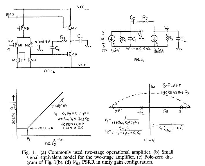
这个传统的miller compensation的问题有两个:
无法驱动很大的电容负载:The op amp stability is severely degraded for capacitive loads of the same order as compensation capacitor (CL must be less than gM2CC/g~l to avoid second pole crossover of the unity gain frequency)。
当power mos是nmos的时候,miller造成的zero会严重影响PSRR的性能:In case of p-channel MOS transistors for the input differential stage, the negative power supply displays a zero at the dominant pole frequency of the op amp in unity gain configuration. This results in serious performance degradation for sampled data systems which use high-frequency switching regulators to generate their power supplies. (In the case of n-channel MOS transistors for the input differential pair, it is the positive supply which shows similar degradation.) This is illustrated in Fig. l(d)。
然后,这个compensation的idea就是除去这个可以short第一级output和第二级output。下面的内容大家不想看可以略去。
The technique is based on removing the feed forwardpath from the first stage output to the op amp output. The circuit shown in Fig. 1 has a current CCd(V. – Vl)/dt flowing into the first-stage output. If one can devise a circuit where only CCdVO/dt current flows into the first stage output, one would have eliminated the feedforward path while still producing a dominant pole due to the Miller effect. The only difference is that Miller capacitance is now AICCrather than (1+ AZ) CCwhere A~is the secondstage voltage gain. Thus, the conceptual ac equivalent of such a circuit is shown in Fig. 2(a)。 Here the compensation capacitor is shown to be connected between the output node and a virtual ground (or ac ground), while the controlled current source having the same value as CCdVo/dt charges the first-stage output. It can be shown that for such an arrangement, the open-loop gain of the op amp is given by
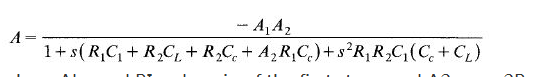
where Al = g~l RI = dc gain of the first stage and A2 = gm2Rz = clc gain of the second stage.
Fig. 2(b) shows its pole-zero location. Notice that there is no finite zero in this circuit and that both the poles are real and are widely spaced.
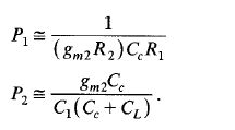
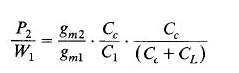
Assuming the internal node capacitance Cl being much smaller than the compensation capacitor CCor the load capacitance CL, the unity gain frequency WI is still given by g~l/CC. This results in
Taking some typical design values of a two-stage amplifier as given by
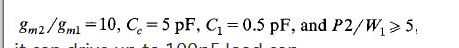
it can drive up to 100pF load cap.
another advantage is:
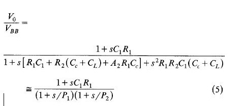
which indicates that is has the same poles as the open-loop gain and a zero which is created by the parasitic capacitance at the first-stage output. Thus, in a unity gain configuration, the VBB PSRR is given by
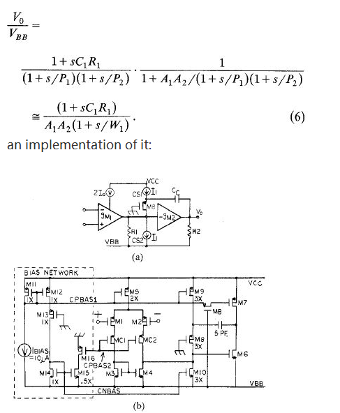
重新贴一下我的电路:
A: nomarl miller (direct,红色Cc0), 1.5pF
B: modified miller (indirect,蓝色Cc和绿色C1): 8pF and 4pF
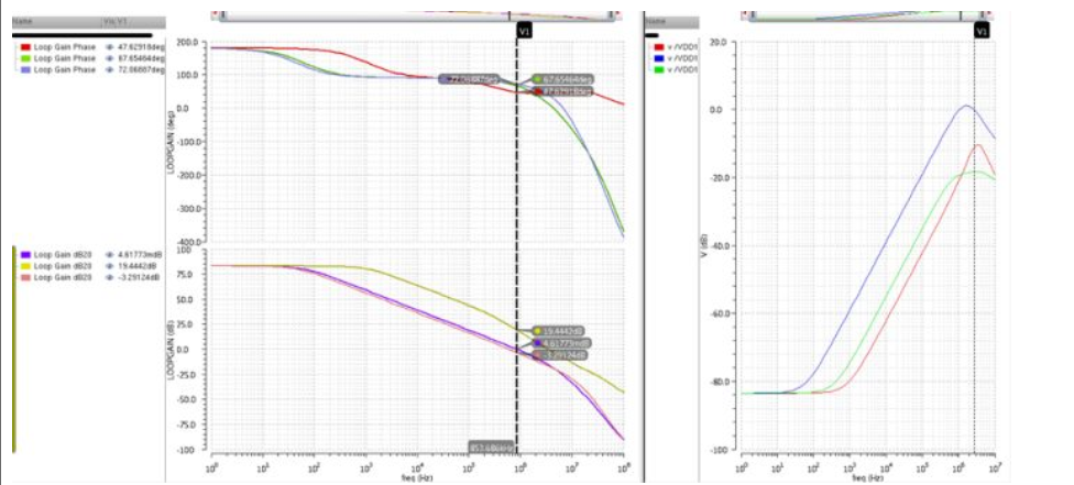
最后比较了一下使用这个compensation之后的PSRR:果然可以很显著的把1MHz那里的peak压下去。比如绿色的那根线,peak被压到了-20dB了。
我们还可以再确认一下,到底dominant pole是不是在那个compensation cap的左边(或者已经可以从PSRR看出来),作者君又改了一下那个Cc的值,得到了下面的loop gain:Cc=0.4pF or 4pF:
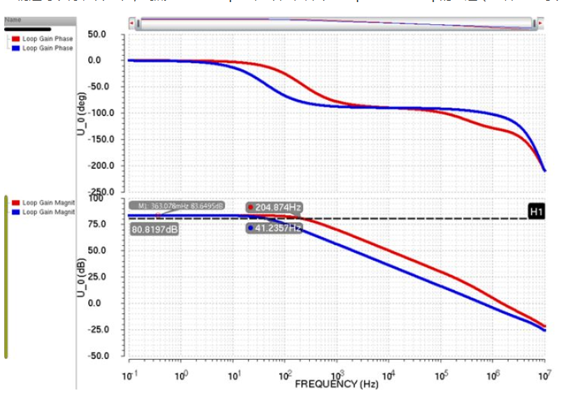
当把Cc从4pF(蓝色)变成0.4pF(红色)之后,明显看到dominant pole往外移动了。